Collaborative research demonstrates unprecedented degree of control over propagation of light waves to perform machine-learning computations
News Highlights:


- New Paper published in Nature Physics introduces a lithium niobate-based, programmable photonic waveguide, developed in collaboration with Cornell University and Stanford University.
- Combining simple fabrication and spatial complexity, the two-dimensional, first-of-its-kind waveguide provides around 10,000 programmable spatial degrees of freedom.
- In benchmark tests with up to 49 dimensional vectors, the chip classified vowels with 96 percent accuracy and recognized handwritten digits with 86 percent accuracy without any trainable electronic processing.
- This research will drive further efficiencies and performance, support novel studies in advanced photonics, and find potential applications in computation, communications and electronics.
SUNNYVALE, Calif.--(BUSINESS WIRE)--NTT Research, Inc., a division of NTT (TY;9432), today announced that members of its Physics & Informatics (PHI) Lab, in collaboration with Cornell University and Stanford University, have demonstrated a photonic processor whose refractive index can be rewritten across a two-dimensional waveguide to exercise virtually arbitrary control over the propagation of light waves and perform machine-learning computations. Built around a lithium niobate slab waveguide, the device provides about 10,000 programmable spatial degrees of freedom. The researchers implemented all-optical neural-network inference on benchmark tests with up to 49 dimensional vectors in a single pass.
Tatsuhiro Onodera and Martin Stein, research scientist and postdoctoral fellow at NTT Research, respectively, led the research under the supervision of Peter L. McMahon, an associate professor at Cornell University. The paper, “Arbitrary control over multimode wave propagation for machine learning,” was published by leading scientific journal Nature Physics online on Dec. 08, 2025. It will be published in print in the January issue.
“The level of control offered by this new waveguide means that we can make linear optical devices of unprecedented spatial complexity,” said Stein, one of the lead authors. “The device is a first of its kind, allowing us to essentially paint any optical circuitry we want and then redraw it in the blink of a second.” That capability enables the use of a feedback loop to create optical circuitry that would be far too complex to build otherwise. Potential applications include optical computation in datacenters, routing of communication signals, and pre-processing of optical information in cameras, among others.
Simple Fabrication, Spatial Complexity, Benchmark Testing
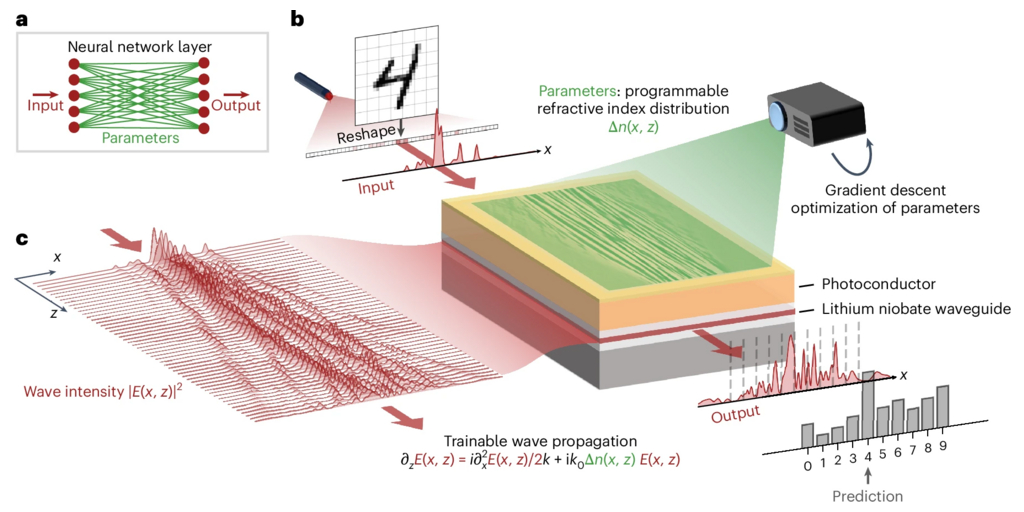
Large-scale photonic devices are conventionally fabricated by combining many discrete components, like phase-shifters and directional couplers. These components need to be isolated from each other, then connected by waveguides and individually controlled by many electrodes. That architecture creates considerable overhead in unused chip area and control systems. The 2D-programmable waveguide developed by NTT Research and its collaborators is much simpler to fabricate and yet permits more spatial complexity. Similar to a pathbreaking silicon nitride-based device recently demonstrated by the same three research organizations, this instance uses a lithium niobate waveguide. (See Figure 1.)
At fabrication, the device is a blank slate—a uniform slab waveguide. It is programmed by projecting illumination patterns that act as virtual electrodes, locally controlling the refractive index in the chip without any physical wiring. Bright regions of the pattern create strong bias voltage across the waveguide and a larger electro-optic response, while dark regions leave the bias voltage unchanged. This arrangement lets a single chip realize many distinct and highly complex linear optical transformations by changing only the illumination pattern.
The team used the chip to perform neural-network inference by training the refractive-index distribution and consequently the multimode wave propagation through the chip. Specifically, they developed a physics-based model of the chip’s behavior, along with a data-driven refinement, allowing the model to be sufficiently accurate to support a backpropagation algorithm introduced four years ago by paper co-authors Onodera, Logan Wright, et al. In machine-learning benchmark tests, the chip performed vowel classification with 96 percent test accuracy and handwritten-digit recognition (MNIST) with 86 percent test accuracy, each in a single optical pass, without trainable digital pre- or post-processing.
Impact on Industry, Performance and Efficiency
The computational and energy costs of deep neural networks (DNNs) associated with machine learning is driven by matrix-vector-multiplications (MVMs). Optical neural networks, particularly those integrated on photonic chips that specialize in performing MVMs with optics instead of electronics, are one promising way to reduce those costs.
According to IDTechEx, the photonic-integrated circuit technology market is projected to experience significant growth over the next decade to over $50 billion in revenue by 2035 (across markets including datacoms, 5G telecoms, quantum, sensors and LiDAR). The technologies developed in this work could address several major obstacles faced by the photonics industry. Instead of manufacturing multiple specialized devices, companies can produce a single programmable chip that performs many functions, potentially reducing R&D and production costs by orders of magnitude. The ability to program functionality after fabrication also means devices can be corrected for manufacturing imperfections, dramatically improving production yields. Finally, single devices performing multiple functions reduce the footprint and complexity of optical systems, with benefits accruing to space and power efficiency.
Spatial efficiency and programmability are primary emphases in this paper. The authors indicate that two-dimensional programmable waveguides may offer not only a constant-factor reduction in device area, but also a scaling benefit, with the area required growing as N1.5 rather than N2. The unprecedented number (10,000) of programmable degrees of freedom translates into richer functionality and higher performance.
The quest for lower energy consumption remains a work in progress. While this device in effect triples the number of dimensional inputs or vectors from a status quo of 16 to 49, that is still below what optics need to deliver an energy-efficient advantage. “If optical computing wants to seriously compete with digital electronic computing, we will need devices that can control hundreds or even thousands of optical modes,” Stein said.
Research Advances PHI Lab Mission
The PHI Lab is a proponent of lithium niobate, a crystalline oxide with nonlinear optical response, strong electro-optical properties and good waveguiding characteristics. (For more, see this video featuring paper co-author and PHI Lab Principal Scientist Timothy McKenna.) In this latest demonstration, the researchers added a distinctive silicon nitride photo-conductor layer to the lithium niobate waveguide.
More broadly, the PHI Lab uses optical technologies as a bridge between advanced information science (classical and quantum) and neuroscience. The concept advanced in this Nature Physics paper will potentially enable the development of reprogrammable photonic simulators supporting both novel studies of bound states in advanced photonics and a wide range of applications in engineering. It may ultimately give rise to a reconfigurable on-chip platform capable of realizing almost every functionality that exists in free-space optics.
About NTT Research
NTT Research opened its offices in July 2019 in Silicon Valley to conduct basic research and advance technologies as a foundational model for developing high-impact innovation across NTT Group’s global business. Currently, four groups are housed at NTT Research facilities in Sunnyvale: the Physics and Informatics (PHI) Lab, the Cryptography and Information Security (CIS) Lab, the Medical and Health Informatics (MEI) Lab, and the Physics of Artificial Intelligence (PAI) Group. The organization aims to advance science in four areas: 1) quantum information, neuroscience and photonics; 2) cryptographic and information security; 3) medical and health informatics; and 4) artificial intelligence. NTT Research is part of NTT, a global technology and business solutions provider with an annual R&D investment of thirty percent of its profits.
###
The names NTT and NTT Research, as well as the NTT and NTT Research logos, are trademarks and service marks of NTT, Inc. or NTT Research, Inc., and/or their affiliates. All other referenced product names are trademarks of their respective owners. © 2025 NTT Research, Inc.
Contacts
NTT Research Contact:
Chris Shaw
Chief Marketing Officer
NTT Research
+1-312-888-5412
chris.shaw@ntt-research.com
Media Contact:
Nick Gibiser
Wireside Communications®
For NTT Research
+1-804-500-6660
ngibiser@wireside.com


